PCB Layout Examples
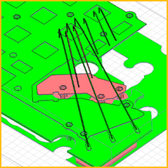
High Speed Layout
Poorly done high speed boards can cost your company tremendous amounts of time and money due to regulatory failures, low manufacturing yields or warranty returns. High speed signals behave like RF signals so incorrect routing techniques can result in a multitude of tribulations. Awareness of the return current path is essential; clocks must have clean edges and skew must be accounted for as well as signal termination and appropriate buss topology.
Comprehension of high speed issues and relevance of common design decisions and trade-off’s results in the best planning and greatest possible success for a high speed project. This is how we do it:
- Identify and prioritize the signals according to their requirements.
- Set budgets for SI, EMU and timing. Then analyze each signal type and determine layout rules that will enable that signal type to meet its budget.
- Choose the layer stack up scheme by simulating.
- Determine a power method which can maintain the objectives.
- Perform a detailed look at termination, ground bounce, ringing, cross talk and EMI and analyze all of the routing needs to determine overall and individual buss rules that will result in a viable board.
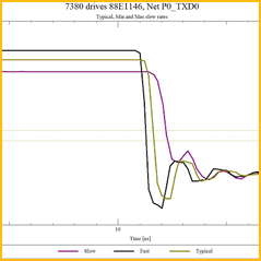
- Route the board and simulate, simulate, simulate to validate that it will meet the budgets.
- Do cross talk analysis to ensure nothing is being coupled causing EMI or other errors.
Rely on our printed circuit board layout proficiency and be more confident in your design.
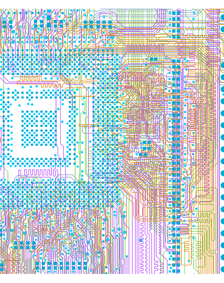
click above to view larger image
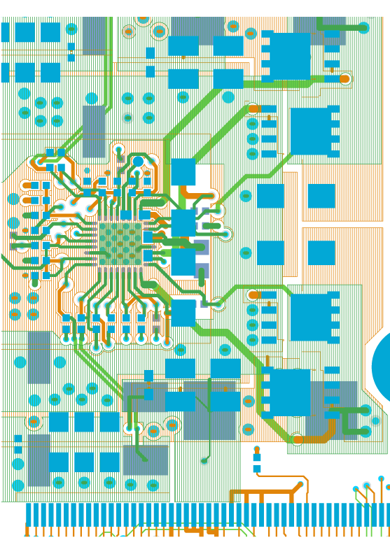
click above to view larger image
Signal Integrity
Did you know that the bulk of re-designs on digital boards are as a result of high speed issues? These issues can begin as digital noise contaminating the analog signals and flow on down in a domino effect to product or regulatory failure.
Signal Integrity Analysis – Characteristic Impedance – Cross-Talk
Board Level Simulation – SSO / Resonance Digital PCB Power

EMI Analysis – Thermal Analysis – Board Material Stack Up Simulations
Design for Manufacture Analysis, FPGA Logic Synthesis
Spectraquest Simulation
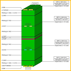
Stackup Impedence Calculations
Wirebond Simulation
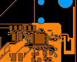
RF & Wireless Layout
Radio Frequency or RF designs are often infamous as “black magic”. This belief exists because the fundamental mechanisms of how RF energy is developed within a printed circuit board is not well understood by many. Many aspects of RF design are theoretical mathematical calculations. An understanding of how this relates to the physical layout world is imperative to a functioning design. During layout, proper design techniques must be used.
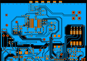
Component Placement
Digital and RF layout techniques can be quite different. One major difference is part placement. Typical digital designs are more forgiving about part placement than RF designs. Digital designs often place components in a similar fashion or orientation, as all vertical or horizontal based on 90 degree rotation increments. RF designs many times use full 360 degree rotational increments so that components can be placed to follow circuit flow. For RF, component location and orientation can be the source of a problem or a cure for how the RF circuit behaves. Many times the rotation of key components in relation to each other can cause an RF circuit to work or fail
Routing
Components are also placed so that there will be minimal lengths for tracing between components. Component pads may be butted up to each other for minimal distances. The lack of defined traces is another significant difference between RF and Digital layouts. RF will utilize globular copper shapes to connect component terminals instead of a defined trace between pads. Physical routes when used generally follow a strip-line or controlled impedance style for connections. The “trace” is referenced to a ground potential or ground plane either on the opposite side or a layer just below in the case of multi-layer designs. Also, there are frequently designed traces or shapes in copper that provide circuit functions as in board trace inductors, couplers or antennas.
Shielding
The use of shielding to contain spurious emissions is also a concern for RF boards. Ground planes can be used to act as image planes or as one side of a PCB-mounted shielded enclosure. PCB shielding is a noninvasive suppression technique that does an outstanding job of reducing both the radiated emissions and susceptibility of a circuit. The use of physical shielding as in radiation shells or cans is another method of containing un-wanted emissions. In some cases the cabinet or enclosure for the circuit board can be made to do double duty and act as the shielding medium.
Other Aspects
Many other details must be factored in when doing RF layouts. Attention as to where circuits are to be located in relation to off board components; overall product design needs; locations for connectors both on board and off board need to be determined for optimal flow as well as interaction with other parts of the product’s design, whether digital or analog to reduce interference issues. Occasionally the use of exotic materials for the RF design needs to be considered. The standard substrate for PCB’s (FR-4) is not always a good choice for all RF circuits.
Good design practices and knowledge can help to keep the bad aspects of that ole “Black Magic” from cropping up.
RoHS Conversions
Pb-free is having some effect on printed circuit board layouts. For Pb-free assemblies, one of the most important layout issues is the component’s physical footprint. It is important to determine whether or not components can resist the higher reflow temperatures needed in the lead-free process. These temperatures can be in excess of 250º or 260ºC. If your existing components can withstand these temperatures then there is no need to select new ones, but if the component can only withstand temperatures around 235ºC, then it is important to replace the component with one that is appropriate for reflow at higher temperatures. If no change to the component, then obviously there is no change in the footprint or layout.
An assembly concern that needs to be considered is whether or not there are SMT components mounted on both sides of the board. The components on the bottom may be glued and must be able to withstand solder temperature of over 250ºC. If they can not, a wave soldering fixture will be needed to shield them.
Additionally, layer stackup and impedance control calculations change if the pcb laminate material is changed to be lead-free complaint. Microstrip, dual stripline or single-ended, these impedances ensure signals get to their destination with minimal crosstalk and as clean as possible so it is important to re-run the calculations on the new chosen material. This can effect a layout globally and require different trace and space for the routing, so don’t underestimate the impact of this on densely routed boards. Materials such as FR406 or FR408 can withstand upwards of 270ºC or higher, but commonly, especially for high-speed boards other materials are required and the calculations using those materials may greatly affect a printed circuit board’s routing.